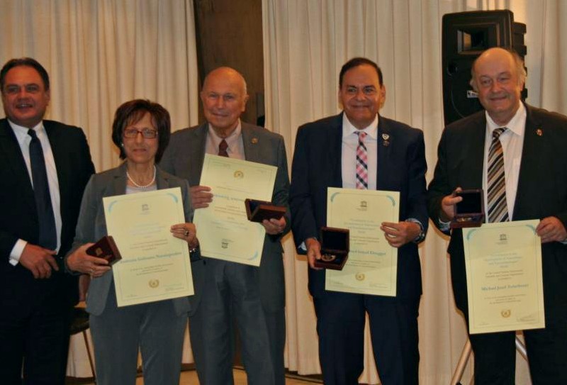
Dr. Androula Nassiopoulou is Director of Research at the Institute of Nanoscience and Nanotechnology (INN) of the National Centre for Scientific Research “Demokritos”, coordinates the Nanoelectrinics, Photonics and Microsystems programme of the Institute and is the Head of the “Nanostructures for Nanoelectronics, Photonics and Sensors” research group. In November 2018 she was honoured with the “UNESCO Medal for outstanding contribution to the development of nanoscience and nanotechnologies” for her research in Si nanostructures for Nanoelectronics and sensors. She was the only woman among the ten recipients of the 2018 Award.
Dr. Nassiopoulou received a B.Sc. degree in Physics from the University of Athens and M.Sc. and Ph.D degrees from the University of Paris XI. She then became Associate Professor at the University of Reims, from where she received the habilitation to direct research in 1985. She joined NCSR Demokritos in 1986 and served as Director of the Centre’s Institute of Microelectronics (IMEL) from 1996 to 2009. Among other distinguished positions, she was also member of the board of Management of NCSR Demokritos in 1996-2009 and Vice President of NCSR Demokritos in 2001-2003, founder and first President of Greek Scientific Society “Micro & Nano” and member of the Governing Board of the European Institute of Nanoelectronics (Sinano), where she is currently Chairperson of the General Assembly.
On the occasion of her recent award, Dr. Nassiopoulou spoke* to Greek News Agenda on the evolution of Nanoscience and Nanotechnology, the practical applications of the Si nanostructures fabricated by her research group and the prospects of this scientific field.
Mrs. Nassiopoulou, you have been recently the recipient of the UNESCO medal for outstanding contribution to Nanoscience and Nanotechnology, an award attributed to few scientists worldwide. How do you feel about this distinction?
UNESCO is the United Nations Organisation for Education and Culture, promoting peace and sustainable development for all, working for establishing the conditions for dialogue among people, civilisations and cultures. Science and Education are two very important pillars towards the above objectives. This is why I feel really honored and proud to be the recipient of an award from that organisation. At the same time I feel that this distinction creates me an obligation to contribute more actively to the above goals. I also believe that this award belongs not only to me, but also to all of my collaborators in research all over the years, to my Research Center NCSR Demokritos in Athens, Greece, but also to my family which always supported me in my work. It is my great pleasure to dedicate this award to all of them.
When did nanotechnology first appear, what does it target and in which fields could it be applied?
The field of Nanoscience and Nanotechnology is a very fast growing cutting-edge field, starting from the early 1990s, with novel applications in all fields of life. It emerged as an expansion of Microelectronics and Integrated Circuit technology, in which the search for faster, lower cost and smaller devices led to today’s very powerful Nanoelectronics technology. This has been achieved by just shrinking the critical size of active devices from the micron to the nanoscale. By reducing the dimensions, tremendous new possibilities in speed and functionality have been opened, based on the very different properties of materials at the nanoscale compared to those of bulk materials. Data processing, transmission of information and storage first profited from the above development. We all followed this revolution the last years in computing and communication systems. When reaching the nanometer scale of active electronic devices, we discovered that all low-dimensional materials – such as nanocrystals, nanofibers or films with nanometer thickness- have completely different properties from those of bulk three-dimensional materials. Differences relate to all their properties, including electrical, dielectric, optical (light emission and absorption, light reflectivity), thermal conductivity and other properties, as well as their compatibility and interaction with living cells and other matter. These new properties opened important new possibilities to design and develop new applications. Thus, a new science and technology branch, called Nanotechnology, came into being, which is a ground-breaking science in which all properties of nanometer-scale materials and devices need to be re-invented. The study and understanding of these new properties and the development of new applications has spread to all areas of human activity. Nanotechnology has been characterised as a cutting-edge enabling technology, which created a new industrial revolution based on high added value products.The first applications concerned information processing and storage technologies (microprocessors, electronic memories), with direct application to our computers and telecommunication systems, but they quickly expanded into a large number of novel devices, including high performance miniaturised sensors, biosensors, medical applications, biology, biotechnology, new complex construction materials with excellent properties, cosmetics, food, transport materials and equipment and in any other application in all fields of life. For the development of the above applications a multidisciplinary approach is necessary, involving scientists from all fields, physicists, chemists, engineers of all disciplines, biologists, biotechnologists, doctors and many others.
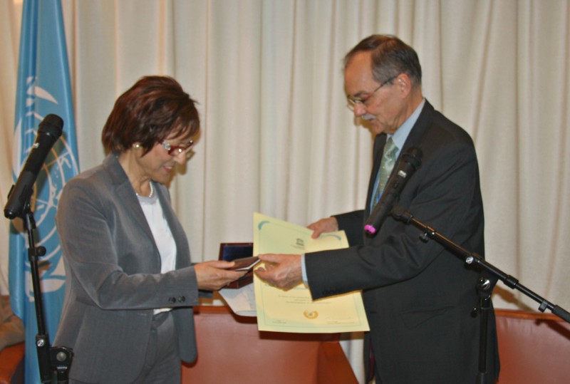 Dr. Nassiopoulou receives the UNESCO Medal
Together with your research group you were the first to develop Si nanowires, as well as innovative nanotechnology applications based on them. Could you explain us how useful these materials and devices are and where do they find applications?
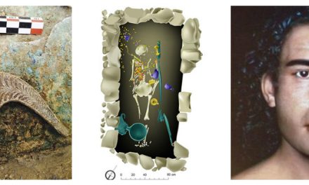
In 1990, Leigh Canham, a British scientist, discovered that if we create random pores inside crystalline silicon by removing more than 60% of the material (porosity exceeding 60%) the resulting material, composed of a skeleton of interconnected nanowires and nanodots, exhibits intense photoluminescence in the visible range at room temperature. This property does not exist in 3-dimensional crystalline silicon. An enormous interest emerged from this discovery in using this property to develop silicon-based optoelectronic devices, fabricated on the same chip with silicon electronics, which was not possible thus far. In this respect, it was first of all necessary to understand the light emission mechanism from low-dimensional structures. The first European research program dedicated to light emission from silicon was thus submitted in 1992, with many partners around Leigh Canham and his team, including my group and our French collaborators from Grenoble. The first hypothesis was that light emission was due to quantum confinement of charge carriers in the tiny Si nanocrystals and nanowires composing the Si skeleton, which had increased probability to recombine radiatively and emit light. Our task as Greek team was to fabricate model structures (ordered silicon nanowires and nanocrystals in an insulating matrix) with a different technique than that used for porous silicon formation and to study their light emitting properties. This is how we fabricated our first Si nanowires worldwide, using a patterning technique that we developed. By studying their optical properties we discovered that they exhibited also other interesting properties different from those of bulk silicon. For example, porous Si shows a very large surface to volume ratio, which can be functionalised to fabricate different kinds of electronic devices, sensors and bio-sensors. It also exhibits very high electrical resistivity, as well as lower dielectric constant than that of bulk silicon. We used those two last properties to develop a local platform on the silicon wafer for the on-chip integration of efficient radiofrequency waveguides, radio frequency filters and high-performance miniaturised on-chip antennas. Another very interesting property of porous Si and other low-dimensional structures is its very low thermal conductivity compared to that of bulk Si. We used this property to develop silicon thermal sensors with improved performance, as well as efficient thermoelectric generators. Furthermore, we measured very low reflectivity from Si nanowires, used to improve the efficiency of Si photovoltaic devices. Currently we use 3-dimensional silicon surface nanostructuring by silicon nanowires to develop Si-based energy storage micro-devices with increased storage capability, which are very useful in energy autonomous microsystems, in combination with miniaturised energy harvesting devices.
Two characteristic examples of applications we have developed include the breath control system that uses our innovative thermal sensor on nanostructured local silicon substrate, and the air flow control system on a vehicle engine developed and tested in a truck.
To what extent, in your opinion, is European funding used in Greece to support businesses selling nanotechnology products?
There exist many innovative companies in Greece developing nanotechnology products. Some of them are spin-offs of Research Centers and Universities. For example, in the Attica Technology Park Lefkippos of my Research Center NCSR “Demokritos” there are several such spin-offs and start-ups. In general, these companies are very active in European research and development programs, securing important European funding.
What are the achievements of nanotechnology thus far and what can we expect in the future?
In addition to the amazing achievements in information society (computers, mobile phones, smart electronics), nanotechnology products can be found today in applications covering all fields of our daily life. To mention some concrete examples, I will take the case of porous silicon mentioned above and the field of medicine and health care. As I already said, porous silicon exhibits a very large internal surface area compared to its volume. By modifying and functionalizing this surface we can make it reactive to specific biomolecules, and can thus use it to fabricate sensitive biosensors or bioanalytical systems. Porous silicon nanoparticles can be also used as drug carriers in drug delivery systems, due to the fact that porous silicon is both bio-compatible and bio-degradable and dissolves slowly inside the body. This application has been developed for local tumor therapy. It is also an interesting material to be used in osteoplastic, in ocular surgery etc.
Nanotechnology applications are rapidly expanding in areas including the environment, health care and medicine, pharmaceuticals, transport materials, systems and equipment, household appliances, food chain, construction materials, toys and everything else one could imagine, enabling the fabrication of better products and “smarter” systems.
*Interview by Marianna Varvarrigou
Read also via Greek News Agenda: University of Athens Online Courses on Nanotechnology and Nanomedicine; Hellenic Foundation for Research and Innovation to Strengthen Research across Greece; The Nanotechnology Boom in Thessaloniki